Wednesday, January 28, 2015

Light Can Generate Power Lift


Scientists create light foil that can push small objects to the side.
Light function to produce the same power that made the aircraft to fly, as shown by recent studies.

With proper design, uniform flow of light push objects are very small as well as an airplane wing aircraft body raised into the air.

Researchers have long known that the light hitting an object can push the object. That's the thinking behind the solar panel, using radiation for propulsion in space. "The ability of light to push something already known," said co-researcher Grover Swartzlander from Rochester Institute of Technology in New York, as quoted in Science News (05/12/10).

New tricks of light is more attractive than a regular boost: It creates a more complicated force called lift, evidence when a flow in one direction to move an object vertically. Air foil or airfoils generate lift; when the engine propeller rotate and move forward fuselage, wings tilted causing the plane ride.

Foil light is not meant to keep an aircraft remain in the air during a flight from one airport to another airport. But the unity of the tools that are very small it may be used to power the micro-machines, transport particles are very small or even allow methods of steering system on the solar panel.

Optical power lift is "a really neat idea," said physicist Miles Padgett from Glasgow University in Scotland, but terlau early to say how these effects may be utilized. "It may be useful, maybe not. Time will tell."

The light can have an unexpected lift is starting from a very simple question, Swartzlander said, "If we have something shaped wings and we shine a light, what happens?" Modeling experiments showed researchers that an asymmetric deflection of light will create a very stable lift. "So we thought it best to do an experiment," said Swartzlander

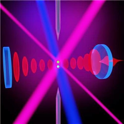
The researchers made a very small bars shaped like an airplane wing, on the one side and flat on the other side winding. When foils micron-sized air is immersed into the water and hit with 130 milliwatts of light from the bottom of the container, foil-foil began to move up, as expected. However, the bars are also began to move to the side, the direction perpendicular to the incoming light. Balls are very small symmetrical lift not show this effect, as the team found.

Different optical power lift from aerodynamic lift with an air foil. An aircraft fly because the air that flows more slowly under his wings using greater pressure than the air flowing faster on. But in light foil, lift created in these objects when the beam through it. Air foil shape transparent stretcher cause refracted light varies depending on where the light was passed, which causes the bending beam within their momentum that generate lift.

The corners of the foil-foil lift this light about 60 degrees, according to the team's findings. "Most objects aerodynamic airs on the corners very gradual, but it has a lift angle remarkable and very strong," said Swartzlander. "You can imagine what would happen if your plane airs at 60 degrees - your stomach will be on foot."

When the bars were lifted, it should not fall or loss of lift, as predicted. "Actually, these objects can stabilize yourself," Padgett said.

Swartzlander said that he hopes to eventually be able to test foils the light in the air as well, and try different shapes and materials with different refraction properties. In the study of the researcher uses infrared light to generate the lift, but other types of light can also, said Swartzlander. "The beautiful thing about this is that it will work as long as you have the light."

The study, published in Nature Photonics on December 5.

Hopefully this can be further investigated and developed for good.

Toward quantum chips: Packing single-photon detectors on an optical chip is crucial for quantum-computational circuits

A team of researchers has built an array of light detectors sensitive enough to register the arrival of individual light particles, or photons, and mounted them on a silicon optical chip. Such arrays are crucial components of devices that use photons to perform quantum computations.

Single-photon detectors are notoriously temperamental: Of 100 deposited on a chip using standard manufacturing techniques, only a handful will generally work. In a paper appearing today in Nature Communications, the researchers at MIT and elsewhere describe a procedure for fabricating and testing the detectors separately and then transferring those that work to an optical chip built using standard manufacturing processes.

In addition to yielding much denser and larger arrays, the approach also increases the detectors' sensitivity. In experiments, the researchers found that their detectors were up to 100 times more likely to accurately register the arrival of a single photon than those found in earlier arrays.

"You make both parts -- the detectors and the photonic chip -- through their best fabrication process, which is dedicated, and then bring them together," explains Faraz Najafi, a graduate student in electrical engineering and computer science at MIT and first author on the new paper.

Thinking small
According to quantum mechanics, tiny physical particles are, counterintuitively, able to inhabit mutually exclusive states at the same time. A computational element made from such a particle -- known as a quantum bit, or qubit -- could thus represent zero and one simultaneously. If multiple qubits are "entangled," meaning that their quantum states depend on each other, then a single quantum computation is, in some sense, like performing many computations in parallel.

With most particles, entanglement is difficult to maintain, but it's relatively easy with photons. For that reason, optical systems are a promising approach to quantum computation. But any quantum computer -- say, one whose qubits are laser-trapped ions or nitrogen atoms embedded in diamond -- would still benefit from using entangled photons to move quantum information around.

"Because ultimately one will want to make such optical processors with maybe tens or hundreds of photonic qubits, it becomes unwieldy to do this using traditional optical components," says Dirk Englund, the Jamieson Career Development Assistant Professor in Electrical Engineering and Computer Science at MIT and corresponding author on the new paper. "It's not only unwieldy but probably impossible, because if you tried to build it on a large optical table, simply the random motion of the table would cause noise on these optical states. So there's been an effort to miniaturize these optical circuits onto photonic integrated circuits."

The project was a collaboration between Englund's group and the Quantum Nanostructures and Nanofabrication Group, which is led by Karl Berggren, an associate professor of electrical engineering and computer science, and of which Najafi is a member. The MIT researchers were also joined by colleagues at IBM and NASA's Jet Propulsion Laboratory.

Relocation
The researchers' process begins with a silicon optical chip made using conventional manufacturing techniques. On a separate silicon chip, they grow a thin, flexible film of silicon nitride, upon which they deposit the superconductor niobium nitride in a pattern useful for photon detection. At both ends of the resulting detector, they deposit gold electrodes.

Then, to one end of the silicon nitride film, they attach a small droplet of polydimethylsiloxane, a type of silicone. They then press a tungsten probe, typically used to measure voltages in experimental chips, against the silicone.

"It's almost like Silly Putty," Englund says. "You put it down, it spreads out and makes high surface-contact area, and when you pick it up quickly, it will maintain that large surface area. And then it relaxes back so that it comes back to one point. It's like if you try to pick up a coin with your finger. You press on it and pick it up quickly, and shortly after, it will fall off."
With the tungsten probe, the researchers peel the film off its substrate and attach it to the optical chip.

In previous arrays, the detectors registered only 0.2 percent of the single photons directed at them. Even on-chip detectors deposited individually have historically topped out at about 2 percent. But the detectors on the researchers' new chip got as high as 20 percent. That's still a long way from the 90 percent or more required for a practical quantum circuit, but it's a big step in the right direction.

Story Source:The above story is based on materials provided by Massachusetts Institute of Technology. The original article was written by Larry Hardesty. Note: Materials may be edited for content and length.
Journal Reference:Ethan A. Englund, Deyun Wang, Hidetsugu Fujigaki, Hiroyasu Sakai, Christopher M. Micklitsch, Rodolfo Ghirlando, Gema Martin-Manso, Michael L. Pendrak, David D. Roberts, Stewart R. Durell, Daniel H. Appella. Programmable multivalent display of receptor ligands using peptide nucleic acid nanoscaffolds. Nature Communications, 2012; 3: 614 DOI: 10.1038/ncomms1629

Improved interface for a quantum internet

Two particles are positioned between highly reflective mirrors and entangled with one another by means of a laser. Additional lasers encode quantum information in the ions and then transfer the information to a single photon.
Credit: U. Innsbruck

A quantum network requires efficient interfaces over which information can be transferred from matter to light and back. In the current issue of Physical Review Letters, Innsbruck physicists led by Rainer Blatt and Tracy Northup show how this information transfer can be optimized by taking advantage of a collective quantum phenomenon.

Quantum computers are no longer just a theoretical concept. In recent years, researchers have assembled and successfully tested the building blocks for a future quantum computer in the laboratory. More than a dozen candidate technologies are currently being studied; of these, ion traps are arguably the most advanced. In an ion trap, single atoms can be confined and precisely controlled by means of lasers. This idea was developed by theorists Ignacio Cirac and Peter Zoller, and a team of Innsbruck experimental physicists under Rainer Blatt has been at the forefront of its implementation. Based at the University of Innsbruck's Institute for Experimental Physics, the team first demonstrated in 2013 that quantum information stored in a trapped ion can be deterministically mapped onto a photon, that is, a quantum of light. Thus, they were able to construct an interface between quantum processors and optical fiber-based communication channels. Now the physicists have improved this interface, making use of so-called superradiant states.

A reliable interface

"In order to build a quantum network with trapped ions, we need an efficient interface that will allow us to transfer quantum information from ions to photons," explains Tracy Northup, project leader in Rainer Blatt's team. "In our interface, we position two ions between two highly reflective mirrors, which form an optical resonator. We entangle the ions with one another and couple both of them to the resonator." The collective interaction between the particles and the resonator can now be tuned in order to enhance the creation of single photons. "This is known as a superradiant state," explains Bernardo Casabone, the article's first author. In order to demonstrate that the interface is well suited for quantum information processing, the researchers encode a quantum state in the entangled particles and transfer this state onto a single photon. Because of the superradiant interaction, the photon is generated almost twice as quickly as in their previous experiment. "Thanks to superradiance, the process of information transfer from the particle to the photon essentially becomes more robust," Casabone emphasizes. As a consequence, the technical requirements for the construction of accurate interfaces may be relaxed.

Read-write capabilities for a quantum memory

In the same experiments on light-matter interactions, the Innsbuck physicists were also able to create so-called subradiant states. Here, the emission of a photon is suppressed rather than enhanced. "These states are also interesting because the stored information becomes invisible to the resonator, and in that sense, it's protected," says Northup. As a result, one can imagine that by switching between sub- and superradiant states, quantum information can be stored in ions and retrieved as photons. In a future quantum computer, such addressable read-write operations may be achieved for a quantum register of trapped ions.
The authors are based at the University of Innsbruck and at the Institute for Quantum Optics and Quantum Information of the Austrian Academy of Sciences. Their research was supported by the Austrian Science Funds (FWF), the European Union, and Tirolean industry.

Story Source:The above story is based on materials provided by University of Innsbruck. Note: Materials may be edited for content and length.
Journal Reference:B. Casabone, K. Friebe, B. Brandstätter, K. Schüppert, R. Blatt, T. E. Northup. Enhanced Quantum Interface with Collective Ion-Cavity Coupling. Physical Review Letters, 2015; 114 (2) DOI: 10.1103/PhysRevLett.114.023602

Rice-sized laser, powered one electron at a time, bodes well for quantum computing

Princeton University researchers have built a rice grain-sized microwave laser.
Credit: Jason Petta, Princeton University

Princeton University researchers have built a rice grain-sized laser powered by single electrons tunneling through artificial atoms known as quantum dots. The tiny microwave laser, or "maser," is a demonstration of the fundamental interactions between light and moving electrons.

The researchers built the device -- which uses about one-billionth the electric current needed to power a hair dryer -- while exploring how to use quantum dots, which are bits of semiconductor material that act like single atoms, as components for quantum computers.
"It is basically as small as you can go with these single-electron devices," said Jason Petta, an associate professor of physics at Princeton who led the study, which was published in the journal Science.

The device demonstrates a major step forward for efforts to build quantum-computing systems out of semiconductor materials, according to co-author and collaborator Jacob Taylor, an adjunct assistant professor at the Joint Quantum Institute, University of Maryland-National Institute of Standards and Technology. "I consider this to be a really important result for our long-term goal, which is entanglement between quantum bits in semiconductor-based devices," Taylor said.

The original aim of the project was not to build a maser, but to explore how to use double quantum dots -- which are two quantum dots joined together -- as quantum bits, or qubits, the basic units of information in quantum computers.

"The goal was to get the double quantum dots to communicate with each other," said Yinyu Liu, a physics graduate student in Petta's lab. The team also included graduate student Jiri Stehlik and associate research scholar Christopher Eichler in Princeton's Department of Physics, as well as postdoctoral researcher Michael Gullans of the Joint Quantum Institute.
Because quantum dots can communicate through the entanglement of light particles, or photons, the researchers designed dots that emit photons when single electrons leap from a higher energy level to a lower energy level to cross the double dot.

Each double quantum dot can only transfer one electron at a time, Petta explained. "It is like a line of people crossing a wide stream by leaping onto a rock so small that it can only hold one person," he said. "They are forced to cross the stream one at a time. These double quantum dots are zero-dimensional as far as the electrons are concerned -- they are trapped in all three spatial dimensions."

The researchers fabricated the double quantum dots from extremely thin nanowires (about 50 nanometers, or a billionth of a meter, in diameter) made of a semiconductor material called indium arsenide. They patterned the indium arsenide wires over other even smaller metal wires that act as gate electrodes, which control the energy levels in the dots.

To construct the maser, they placed the two double dots about 6 millimeters apart in a cavity made of a superconducting material, niobium, which requires a temperature near absolute zero, around minus 459 degrees Fahrenheit. "This is the first time that the team at Princeton has demonstrated that there is a connection between two double quantum dots separated by nearly a centimeter, a substantial distance," Taylor said.

When the device was switched on, electrons flowed single-file through each double quantum dot, causing them to emit photons in the microwave region of the spectrum. These photons then bounced off mirrors at each end of the cavity to build into a coherent beam of microwave light.

One advantage of the new maser is that the energy levels inside the dots can be fine-tuned to produce light at other frequencies, which cannot be done with other semiconductor lasers in which the frequency is fixed during manufacturing, Petta said. The larger the energy difference between the two levels, the higher the frequency of light emitted.
Claire Gmachl, who was not involved in the research and is Princeton's Eugene Higgins Professor of Electrical Engineering and a pioneer in the field of semiconductor lasers, said that because lasers, masers and other forms of coherent light sources are used in communications, sensing, medicine and many other aspects of modern life, the study is an important one.

"In this paper the researchers dig down deep into the fundamental interaction between light and the moving electron," Gmachl said. "The double quantum dot allows them full control over the motion of even a single electron, and in return they show how the coherent microwave field is created and amplified. Learning to control these fundamental light-matter interaction processes will help in the future development of light sources."
The paper, "Semiconductor double quantum dot micromaser," was published in the journal Science on Jan. 16, 2015. The research was supported by the David and Lucile Packard Foundation, the National Science Foundation (DMR-1409556 and DMR-1420541), the Defense Advanced Research Projects Agency QuEST (HR0011-09-1-0007), and the Army Research Office (W911NF-08-1-0189).

Story Source:The above story is based on materials provided by Princeton University. Note: Materials may be edited for content and length.
Journal Reference:Y.- Y. Liu, J. Stehlik, C. Eichler, M. J. Gullans, J. M. Taylor, J. R. Petta. Semiconductor double quantum dot micromaser. Science, 2015; 347 (6219): 285 DOI: 10.1126/science.aaa2501

New pathway to valleytronics: Femtosecond laser used to manipulate valley excitons


A study has shown that the optical Stark effect, which describes the energy shift in a two-level system induced by a non-resonant laser field, can be used to control valley excitons in MX2 semiconductors.

Apotential avenue to quantum computing currently generating quite the buzz in the high-tech industry is "valleytronics," in which information is coded based on the wavelike motion of electrons moving through certain two-dimensional (2D) semiconductors. Now, a promising new pathway to valleytronic technology has been uncovered by researchers with the Lawrence Berkeley National Laboratory (Berkeley Lab).

Feng Wang, a condensed matter physicist with Berkeley Lab's Materials Sciences Division, led a study in which it was demonstrated that a well-established phenomenon known as the "optical Stark effect" can be used to selectively control photoexcited electrons/hole pairs -- referred to as excitons -in different energy valleys. In valleytronics, electrons move through the lattice of a 2D semiconductor as a wave with two energy valleys, each valley being characterized by a distinct momentum and quantum valley number. This quantum valley number can be used to encode information when the electrons are in a minimum energy valley. The technique is analogous to spintronics, in which information is encoded in a quantum spin number.

"This is the first demonstration of the important role the optical Stark effect can play in valleytronics," Feng says. "Our technique, which is based on the use of circularly polarized femtosecond light pulses to selectively control the valley degree of freedom, opens up the possibility of ultrafast manipulation of valley excitons for quantum information applications."
Wang, who also holds an appointment with the University of California (UC) Berkeley Physics Department, has been working with the 2D semiconductors known as MX2 materials, monolayers consisting of a single layer of transition metal atoms, such as molybdenum (Mo) or tungsten (W), sandwiched between two layers of chalcogen atoms, such as sulfur (S). This family of atomically thin 2D semiconductors features the same hexagonal "honeycombed" lattice as graphene. Unlike graphene, however, MX2 materials have natural energy band-gaps that facilitate their use in transistors and other electronic devices.

This past year, Wang and his group reported the first experimental observation of ultrafast charge transfer in photo-excited MX2 materials. The recorded charge transfer time of less than 50 femtoseconds established MX2 materials as competitors with graphene for future electronic devices. In this new study, Wang and his group generated ultrafast and ultrahigh pseudo-magnetic fields for controlling valley excitons in triangular monolayers of WSe2 using the optical Stark effect.

"The optical Stark effect describes the energy shift in a two-level system induced by a non-resonant laser field," Wang says.

"Using ultrafast pump-probe spectroscopy, we were able to observe a pure and valley-selective optical Stark effect in WSe2 monolayers from the non-resonant pump that resulted in an energy splitting of more than 10 milli-electron volts between the K and K? valley exciton transitions. As controlling valley excitons with a real magnetic field is difficult to achieve even with superconducting magnets, a light-induced pseudo-magnetic field is highly desirable."
Like spintronics, valleytronics offer a tremendous advantage in data processing speeds over the electrical charge used in classical electronics. Quantum spin, however, is strongly linked to magnetic fields, which can introduce stability issues. This is not an issue for quantum waves.
"The valley-dependent optical Stark effect offers a convenient and ultrafast way of enabling the coherent rotation of resonantly excited valley polarizations with high fidelity," Wang says. "Such coherent manipulation of valley polarization should open up fascinating opportunities for valleytronics."

Story Source:The above story is based on materials provided by DOE/Lawrence Berkeley National Laboratory. Note: Materials may be edited for content and length.Journal Reference:J. Kim, X. Hong, C. Jin, S.-F. Shi, C.-Y. S. Chang, M.-H. Chiu, L.-J. Li, F. Wang. Ultrafast generation of pseudo-magnetic field for valley excitons in WSe2 monolayers. Science, 2014; 346 (6214): 1205 DOI: 10.1126/science.1258122